

Nanometer Design Challenges in VLSI
Explore challenges in power, performance and scaling.
Read articleLearn with Abhyasa
Explore semiconductor design, verification, industry careers and practical Physical Design guides.
Explore challenges in power, performance and scaling.
Read article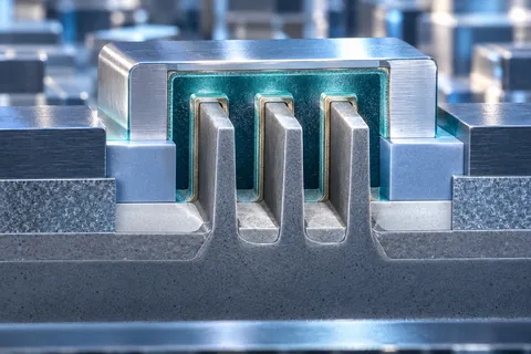
How FinFET transistors enable smaller and more efficient chips.
Read article
Compare Fusion Compiler and Innovus commands.
Read article
Explore chip design, verification and fabrication career paths.
Read article
What engineering students can learn for a career in VLSI.
Read article
Explore six trends shaping electronics engineering, from AI and 5G to sustainable and quantum technologies.
Read article
Understand process variation, leakage, signal integrity and tool challenges at advanced nodes.
Read articleCore utilization, effective utilization, density, row spacing and logical hierarchy.
Read guideUnderstand parasitic thyristors, triggering conditions, well taps and prevention.
Read guideLearn how trimDesign creates a compact, self-contained block in Innovus.
Read guideCompare guide, fence, region and cluster constraints in physical design.
Read guide