Understanding FinFET Technology in VLSI
Learn how FinFET transistors are revolutionizing VLSI design, enabling smaller, faster, and more efficient chips.
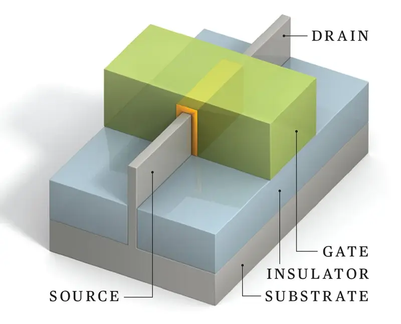
As technology demands more efficient, high-performance devices, the limitations of traditional planar transistors have led to a pivotal innovation: FinFET (Fin Field-Effect Transistor) technology. FinFETs mark a major shift in Very-Large-Scale Integration (VLSI) design, introducing a three-dimensional structure that allows for better control over electrical current, especially at the small geometries required in modern electronics. In this blog post, we’ll break down what makes FinFETs unique and why they’re crucial for advancing VLSI. Unlike conventional MOSFETs, which are limited to a flat, two-dimensional plane, FinFETs utilize a fin-shaped, vertical channel that improves gate control. This design effectively reduces issues like leakage current and short-channel effects, which are common at the sub-20nm scale. With FinFETs, devices achieve faster speeds, lower power consumption, and greater scalability, making this technology ideal for power-sensitive applications such as smartphones, wearables, and high-performance computing. We’ll also explore the challenges associated with FinFET implementation in VLSI, including design complexity, manufacturing considerations, and the specialized techniques engineers use to maximize FinFET efficiency. Finally, we’ll look at how FinFET technology has opened doors to more advanced transistor designs, driving innovation in IoT, AI, and other rapidly evolving fields. This post is ideal for anyone interested in understanding the latest advancements in VLSI and how FinFET technology is shaping the future of semiconductor design. Whether you’re an industry professional or a student, this blog offers a clear, in-depth look at the transformative impact of FinFET technology on modern electronics.