Latch-Up in CMOS/BiCMOS Circuits: Causes, Impact, and Prevention
Understanding and mitigating latch-up in CMOS/BiCMOS circuits is crucial for reliable circuit design.
What is Latch-Up?
Latch-up is an undesirable phenomenon in CMOS and BiCMOS circuits, where a low-impedance path forms between the power supply (VDD) and ground (GND). This condition can result in excessive current flow, potentially leading to system failure or permanent damage to the circuit.
Causes of Latch-Up
Latch-up occurs due to regenerative feedback between the parasitic PNP and NPN transistors that inherently exist in CMOS technology. These parasitic transistors form an unintended Silicon-Controlled Rectifier (SCR) or Thyristor structure, which can be inadvertently triggered under certain conditions.
Impact of Latch-Up on Circuit Design
The parasitic PN junctions in CMOS structures can form an SCR, causing an unexpected short circuit between VDD and GND. A significant input current can trigger this SCR, leading to self-sustaining conduction and potential thermal runaway. If not mitigated, latch-up can result in permanent device damage, power failure, or system instability.
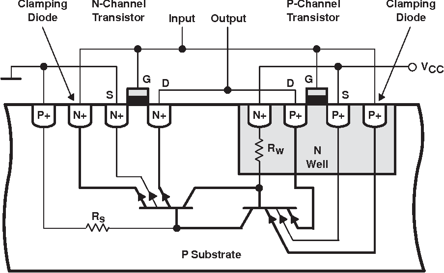
Internal Structure Leading to Latch-Up
Parasitic Transistors Formation
NPN Transistor: Emitter: Drain/source of the N-channel MOSFET; Base: P-substrate; Collector: N-well containing the complementary P-channel MOSFET
PNP Transistor: Emitter: Drain/source of the P-channel MOSFET; Base: N-well containing the complementary P-channel MOSFET; Collector: P-substrate
Thyristor/SCR (PNPN Diode) Structure: Anode: Drain/source of the P-channel MOSFET; Cathode: Drain/source of the N-channel MOSFET; Gate: P-substrate
Triggering of the Latch-Up Mechanism
- Voltage Spikes: Sudden voltage transients that forward bias the parasitic junctions.
- ESD (Electrostatic Discharge): Excessive charge injection during handling or operation.
- Radiation Effects: Charge buildup in space and high-energy environments.
- High Substrate/WELL Resistance: Increased resistance between the substrate and supply rails.
Prevention and Remedies for Latch-Up
Process-Level Solutions:
- Latch-Up Resistant CMOS Process: Use a thin epitaxial layer on top of a highly doped substrate to reduce parasitic transistor gain. Increase the holding voltage above the VDD supply voltage to prevent SCR activation. Use a retrograde well structure, where the bottom is highly doped, and the top is lightly doped.
- Well and Substrate Engineering: Increase dopant concentration of the substrate and well to lower the gain of parasitic transistors. Maintain a trade-off since higher doping can lead to an increase in threshold voltage (VT).
Layout and Design-Level Solutions:
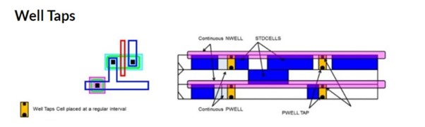
- Well Tap and Substrate Contacts Placement: Reduce well and substrate resistance (RS and RW) by keeping substrate and well contacts close to transistor source connections. Place well taps at regular intervals to maintain a uniform potential across the substrate and wells.
- Guard Rings Implementation: Surround sensitive areas with guard rings to absorb injected charges and prevent triggering of latch-up. Widely used in analog designs to minimize the gain of parasitic transistors.
- Standard Cell-Based Design Considerations: Standard cells do not have internal well taps to reduce design complexity, requiring external well tap cells sprinkled across the core area. The placement density of well taps is determined by the foundry specifications to balance resistance reduction and core area utilization.
Physical Design Considerations: End-Cap Cells
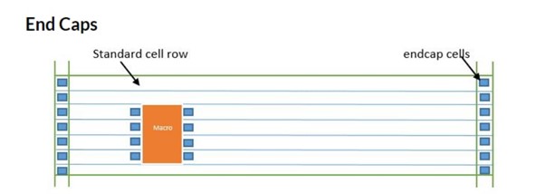
End-cap cells are preplaced physical-only cells that help meet design rules and prevent gaps in well and implant layers, ensuring well continuity. They connect only to power and ground rails once the power rails are created. Prevent Design Rule Check (DRC) violations by ensuring well tie-off requirements are met. Are placed at the left and right ends of the core rows and in fragmented core rows to maintain continuity. End-cap cells are fixed and cannot be moved during optimization.
Trade-Off in Tap and End-Cap Cell Placement
More tap cells reduce well/substrate resistance, mitigating latch-up but increasing core area utilization. A well-balanced approach is provided by foundry guidelines, ensuring optimal placement of tap and end-cap cells.
Conclusion
Latch-up is a critical reliability concern in CMOS/BiCMOS designs, but effective process, layout, and design techniques can significantly reduce its occurrence. By implementing proper well tap placement, guard rings, and optimized doping strategies, designers can enhance circuit robustness against latch-up failures.